Silicon for ultra-broadband, ultra-fast and low-energy optical signal processing
We want to unearth the most efficient nonlinear integrated photonics platform capable of multi-terabit optical signal processing.
In order to do this we will explore the:
- Best materials compatible with silicon substrates.
- Best structures for different applications.
- Best processing technology to get ultra-low linear loss.

Materials
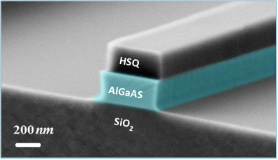
High nonlinearity and low multiphoton absorption (two-photon absorption (TPA), three-photon absorption (ThPA),…) are key to the objectives of the flagship. Crystalline silicon is TPA free above 2.2 µm and is an extremely good material in this range. In the standard telecom 1.55 µm wavelength range other materials will be needed as the non-linear medium and e.g. AlGaAs can be tailored to have no TPA due to a bandgap larger than double the photon energy. Going further, materials like silicon nitride, silicon carbide, gallium nitride, aluminum nitride, titanium oxide, zinc oxide, lithium niobate and diamond are even without ThPA while retaining a fairly high non-linearity. Nanostructured materials like amorphous silicon or silicon nanoclusters are also candidates offering low TPA and high material nonlinearity. In all cases it is important that the materials can be deposited on large area silicon substrates to be compatible with the emerging silicon photonics industry employing depreciated CMOS fabs. We will investigate a number of these materials and also try to get a deeper understanding of the influence of the internal structure of the materials (crystalline, nanocrystalline, amorphous) on the nonlinear performance including parasitic processes resulting in crosstalk and noise.
Structures
Due to a high index contrast and wavelength scale waveguide dimensions it is possible to tailor dispersion (e.g. nanowire) or field confinement (e.g. slot waveguide) to maximize the wideband non-linearity. Also, resonant structures (microrings, cavities, gratings etc.) can enhance nonlinearities although at a tradeoff with bandwidth. In some cases there may not be an ideal materials for all the functionalities which we want to achieve and proper material combinations key. We can also use structures to counter detrimental material properties e.g. using electrodes on silicon for carrier sweep-out to minimize free carrier absorption which is a side-
effect of the multiphoton absorption.
Processing technology
Surface roughness on the nanometer scale is determining most of the linear loss for the devices and control at this scale is extremely challenging and important. Intricate process-optimizations allows minimizing the roughness but every material will need separate optimization to achieve the performance we need.
Terabit/s experiments
Our terabit/s test bed will be used to understand the limitations of the materials and structures. Time lens, phase-sensitive processes, noise studies, and other
system scenario investigations will be integral to the characterization and unique for the center.